HiFi4 Boot Loader and Memory Map
This section provides an overview of:
HiFi4 Boot Loader
For better power efficiency, by default the HiFi4 DSP is powered off when RT6xx powers up. To boot up, Cortex M33 acts as master core to configure DSP local memories, clocks, load DSP images, and so on. SDK has wrapped up this part as HiFi4 Boot Loader or the DSP driver. The essentials are located in: <SDK path>\devices\MIMXRT685S\drivers\fsl_dsp.h & fsl_dsp.c.
For each DSP example, it also provides two more implementation files for detailed configurations: <SDK path>\boards\evkmimxrt685\dsp_examples\<any dsp example>\cm33\dsp_support.h & dsp_support.c
Below is the DSP boot procedure with more elaborations.
To run DSP at full power, for example, 600 MHz, SoC Vddcore is set to 1.1 V. If full power is not required, for example, to run DSP at the half speed at 300 MHz, then Vddcore only requires 0.8 V. RT6xx EVK integrates NXP PCA9420 PMIC for power management and by default Vddcore is set to 1.0 V.
Therefore, PMIC is initialized for better power management. For details on Vddcore and DSP frequency operating conditions, see any dsp example\cm33\pmic_support.c BOARD_SetPmicVoltageForFreq(), or see the data sheet, section 13.1, General Operating Conditions.
/* Initialize PMIC PCA9420 */
BOARD_InitPmic();
/* Configure PMIC Vddcore value according to main/dsp clock. */
BOARD_SetPmicVoltageForFreq(CLOCK_GetMainClkFreq(), CLK_600MHZ);
It is possible to clock DSP from various clock sources. The DSP PLL for full power and can also run at FFRO low-frequency clocks to save the power.
/* Enable DSP PLL clock 594MHz. */
CLOCK_InitSysPfd(kCLOCK_Pfd1, 16);
/*Let DSP run on DSP PLL clock with divider 1 (594Mhz). */
CLOCK_AttachClk(kDSP_PLL_to_DSP_MAIN_CLK);
CLOCK_SetClkDiv(kCLOCK_DivDspCpuClk, 1);
As Cortex M33 and SRAM are clocked at lower speed/ max frequency at 300 MHz, set the DSP AHB bus clock divider as 2.
CLOCK_SetClkDiv(kCLOCK_DivDspRamClk, 2);
If DSP clock is running at 300 MHz or lower, it is more efficient to use divider as 1. For divider as 1, note that an extra register SYSCTL0_PACKERENABLE is set. For more details, see the user manual section 4.5.2.18 DSP Main Ram Clock Divider and section 4.5.5.3 Packer Enable.
/* This is a quick register setting example for secure mode */
/* SYSCTL0->PACKERENABLE = 0x4 */
Power up TCM/ DSP local memories and cache, supply clock, and reset peripherals.
/* Initializing DSP core */
DSP_Init();
For SDK DSP examples, split the DSP images into three parts.
One is for vectors and critical sections sitting on TCM/ DSP local memories. The second one is for normal code and data sections sitting on SRAM, and the final is for non-cached DSP initialized data in SRAM.
Here, Cortex M33 load those binaries to its destination. When the DSP program is debugged, it is possible to load DSP binaries from the Xtensa Xplorer IDE, as described in Prepare DSP Core for ‘Hello World’. To load binaries, remove the DSP_IMAGE_COPY_TO_RAM compilation flag or set it to 0. By default, the compilation flag is set to 1 and always load the DSP images.
#if DSP_IMAGE_COPY_TO_RAM
    /* Copy application from RAM to DSP_TCM */
    DSP_CopyImage(&tcm_image);
    /* Copy application from RAM to DSP_RAM */
    DSP_CopyImage(&sram_image);
    /* Copy application from RAM to DSP_Uncached RAM */
    DSP_CopyImage(&ncache_image);
#endif
The DSP stall register SYSCTL0_DSPSTALL controls the HiFi4 operation. Start the DSP and run it.
/* Run DSP core */
DSP_Start();
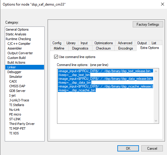
The post build scripts create the DSP images. For details, see Makefile.include in any DSP example. To reduce the image size and make image copy more efficient, they are split into SRAM part; TCM part, and uncached SRAM part. DSP images are set and linked into Cortex M33 side. For IAR, the linker is set in Project Options > Linker > Extra Options. For ArmGCC or Linux environment, set in any DSP example\cm33\incbin_gcc.S.
|
|
Parent topic:HiFi4 Boot Loader and Memory Map
Linker and Memory Map
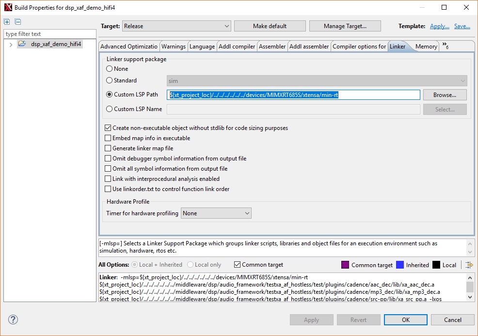
When importing the SDK DSP examples, by default the mode is set as Release. The default mode means that the images must be built in Release mode with ‘min-rt’ Linker Support Package/ LSP. To double-check, open SDK DSP examples > Build Properties > Linker.
|
|
SDK provides three different LSPs.
‘min-rt’ for Release mode - ‘min-rt’ eliminates all unnecessary debug info and reduces image size.
‘gdbio’ for Debug mode - gdbio’ support standard ‘printf’/ log output back to Xtensa Xplorer debug console, as well as other debug utilities, perfect for debug purpose but not appropriate for official deployment nor loading directly from Cortex M33 side.
‘sim’ for simulations - ‘sim’ only works for software simulation and does not fit on device debugging.
The memory map is identical for different LSPs. It sits with linker scripts in SDK path\devices\MIMXRT685S\xtensa\’LSP name’\ldscripts\elf32xtensa.x. It specifies how HiFi4 DSP organizes image sections on the memory. For example:
0x0020 0000 ~ 0x0048 0000, size 2.5 M bytes, for code and data.
Stack and Heap are at the top of the segment and count top down from 0x0048 0000 to lower.
0x2400 0000 ~ 0x2400 FFFF, size 64 K bytes, for Data TCM. By default, it is empty.
0x2402 0000 ~ 0x2402 FFFF, size 64 K bytes, for instruction TCM. By default it only contains essential vectors and left around 62 K for applications.
0x2004 0000 ~ 0x2007 FFFF, size 256 K bytes. This is non-cached area for Cortex M33 and HiFi4 DSP data exchange.
Note that both Cortex M33 and HiFi4 DSP have access to all SRAM partitions. It means that a unified memory map is necessary at system level and both cores must not affect each other’s memory map. For SDK examples, see that HiFi4 memory map starts from 0x0020 0000 and Cortex M33 side sits under this address. Using IAR environment, as an example, its memory map sits in SDK path\boards\evkmimxrt685\dsp_examples\ any example\cm33\iar\MIMXRT685Sxxxx_ram.icf.
0x0008 0000 ~ 0x0017 FFFF, for interrupt vectors and code.
0x0018 0000 ~ 0x001F FFFF, for data.
The memory map is flexible and can be adjusted as per the requirement of the application. Note that modifying the core’s memory map might affect another. Changes to both the cores must be made accordingly. For example, when allocating more SRAM partitions to DSP, you must reduce the memory taken at Cortex M33 side. Otherwise, Cortex M33 might not work properly. Also, when loading DSP image directly from Cortex M33 side, the image still sits in Cortex M33 data section before booting up. Therefore, it raises the bar for application data section requirements. You may consider running the application from FLASH.
Parent topic:HiFi4 Boot Loader and Memory Map
Cache and Data Exchange Memory Partitions
You may have noticed that HiFi4 DSP has a small non-cached area that starts from 0x20040000. The non-cached are used for data exchange between two cores. As both M33 and HiFi DSP have shared access to all SRAM partitions, shared memory access is the most effective way to exchange data between two cores. The given physical addresses are read/ written by both cores at same address, no memory mapping or address converting is required. For example, if a piece of data array is passed from Cortex M33 to HiFi4 DSP, only the start pointer and the size of the array is passed, and conversely. It is convenient for system programming and simplifies the inter-core communications.
Consider cache here. Cortex M33 has no cache, the entire SRAM is considered as its local memory. Therefore, any memory write is flushed immediately. HiFi4 has 32 K instruction cache and 64 K data cache, and both cache are enabled by default. Therefore, the memory write is not flushed immediately. To make a tradeoff between performance and IPC convenience, set the non-cached area for data exchange memory partitions.
The above memory map has specified the non-cached region, and in DSP code, and HAL functions are called to disable the cache. For details, see the audio framework example in SDK path\boards\evkmimxrt685\dsp_examples\xaf_demo\dsp\xaf_main_dsp.c. For more details about HAL cache function, see the Xtensa System Software Reference Manual, section 3.11 Cache
/* Disable DSP cache for RPMsg-Lite shared memory. */
xthal_set_region_attribute((void *)RPMSG_LITE_SHMEM_BASE, RPMSG_LITE_SHMEM_SIZE, XCHAL_CA_BYPASS, 0);
/* Disable DSP cache for noncacheable sections. */
xthal_set_region_attribute((uint32_t *)&NonCacheable_start,
                               (uint32_t)&NonCacheable_end - (uint32_t)&NonCacheable_start, XCHAL_CA_BYPASS, 0);
Note that the XHAL call sets cache attribute of the whole region/ 512 M bytes even if the set size is passed. This is also one reason why non-cached attribute is set on the overlapping SRAM address and starts from 0x2000 0000. This also distinguished the physical SRAM addresses starting from 0x0000 0000, which is cacheable area for HiFi4.
Data exchange memory partitions are flexible and can be configured as per application’s requirement. However, to mitigate the possible AHB arbitration between the two cores, use of the first eight 32 K and following four 64 K memory partitions is recommended. DSP Data TCM is also used as data exchange area for those data have high demand on timing performance. You must avoid accessing same partition at same time for frequent data exchange between two cores. You can keep one core in Sleep or Wait for Interrupt while another core operating, or set up a ping pong data exchange/ DMA such that when one core fills one partition, another core fetches another partition, and conversely.
For more details about the RT6xx memory map, see the user manual, section 2 Memory Map, and section 2.1.11 HiFi4 memory map.
Parent topic:HiFi4 Boot Loader and Memory Map
Boot or Run from Flash
Boot from Flash is straight forward when using IAR environment. SDK provides either two or four different build configurations based on the project: debug (from SRAM)/ release (from SRAM)/ flash_debug/ flash_release. Flash configurations use different memory map in project linker options. For details, see Figure 1.
|
|
To enable booting from flash, change the ISP mode/ SW5 switches on the EVK.
If using MCUXpresso/ armgcc build environment, note that by default build environment is set to boot from flash. Using MCUXpresso as an example:
Make sure to use the latest version of MCUXpresso.
Import the SDK examples.
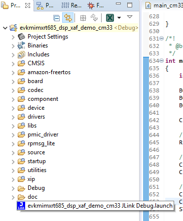
Once completed, double click the last file/ J-Link Debug.
|
|
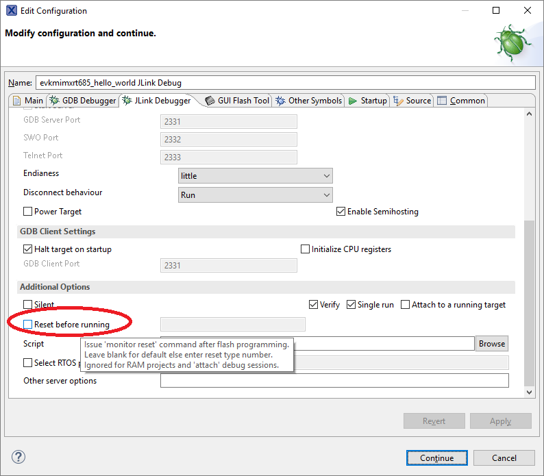
Launch to modify J-Link debugger setting.
Make sure to deselect Reset before running. This helps the flash-based program get into main function.
|
|
Make sure to:
Modify DSP_IMAGE_COPY_TO_RAM and Define to 1 in Project settings > C/C++ General > Paths and Symbols > Symbols.
Have the right compilation flag as C/C++. Compilation flags do not work on *.S files.
Have #define DSP_IMAGE_COPY_TO_RAM 1 as the first line of source/incbin.S to include the DSP binaries.
Use the correct DSP binaries at correct path (must be release binaries).
Provide the right image path to incbin.S.
To run/boot from flash, make sure that the board is set to FlexSPI flash boot mode (ISP2: ISP1: ISP0 = ON, OFF, ON).
Parent topic:HiFi4 Boot Loader and Memory Map
Parent topic:HiFi4 System Programming