HiFi4 System Programming
This section provides more examples, tips, and some best practices about HiFi4 programming on RT600 EVKs. It focuses more on RT6xx and SDK. For general HiFi programming, see the Xtensa IDE documents. You can find them in the directory Xtensa Xplorer IDE menu Help > PDF Documentation.
The following are some frequently used references:
Xtensa Instruction Set Architecture (ISA) Reference Manual: Architecture/ high-level overview.
HiFi 4 DSP User’s Guide: Most useful reference manual for DSP programmer. It has all details about HiFi4 instructions and intrinsics, as well as some algorithm optimization techniques.
Xtensa XOS Reference Manual: XOS is the default and native embedded kernel for Xtensa HiFi cores. SDK examples use XOS as well.
Xtensa System Software Reference Manual: XTOS, also known as the basic runtime and handlers, has been depreciated and moved toward XOS. However, the Xtensa Processor Hardware Abstraction Layer/ HAL is still very useful in many perspectives. SDK examples use HAL functions.
Xtensa Linker Support Packages (LSPs) Reference Manual and GNU Linker User’s Guide: Both documents are useful for understanding the HiFi program linker and the memory map.
Specifically for RT6xx, the user manual and the data sheet are the most important references. All product specifications are found in the user guide and data sheet documents.
HiFi4 Boot Loader and Memory Map
This section provides an overview of:
HiFi4 Boot Loader
For better power efficiency, by default the HiFi4 DSP is powered off when RT6xx powers up. To boot up, Cortex M33 acts as master core to configure DSP local memories, clocks, load DSP images, and so on. SDK has wrapped up this part as HiFi4 Boot Loader or the DSP driver. The essentials are located in: <SDK path>\devices\MIMXRT685S\drivers\fsl_dsp.h & fsl_dsp.c.
For each DSP example, it also provides two more implementation files for detailed configurations: <SDK path>\boards\evkmimxrt685\dsp_examples\<any dsp example>\cm33\dsp_support.h & dsp_support.c
Below is the DSP boot procedure with more elaborations.
To run DSP at full power, for example, 600 MHz, SoC Vddcore is set to 1.1 V. If full power is not required, for example, to run DSP at the half speed at 300 MHz, then Vddcore only requires 0.8 V. RT6xx EVK integrates NXP PCA9420 PMIC for power management and by default Vddcore is set to 1.0 V.
Therefore, PMIC is initialized for better power management. For details on Vddcore and DSP frequency operating conditions, see any dsp example\cm33\pmic_support.c BOARD_SetPmicVoltageForFreq(), or see the data sheet, section 13.1, General Operating Conditions.
/* Initialize PMIC PCA9420 */
BOARD_InitPmic();
/* Configure PMIC Vddcore value according to main/dsp clock. */
BOARD_SetPmicVoltageForFreq(CLOCK_GetMainClkFreq(), CLK_600MHZ);
It is possible to clock DSP from various clock sources. The DSP PLL for full power and can also run at FFRO low-frequency clocks to save the power.
/* Enable DSP PLL clock 594MHz. */
CLOCK_InitSysPfd(kCLOCK_Pfd1, 16);
/*Let DSP run on DSP PLL clock with divider 1 (594Mhz). */
CLOCK_AttachClk(kDSP_PLL_to_DSP_MAIN_CLK);
CLOCK_SetClkDiv(kCLOCK_DivDspCpuClk, 1);
As Cortex M33 and SRAM are clocked at lower speed/ max frequency at 300 MHz, set the DSP AHB bus clock divider as 2.
CLOCK_SetClkDiv(kCLOCK_DivDspRamClk, 2);
If DSP clock is running at 300 MHz or lower, it is more efficient to use divider as 1. For divider as 1, note that an extra register SYSCTL0_PACKERENABLE is set. For more details, see the user manual section 4.5.2.18 DSP Main Ram Clock Divider and section 4.5.5.3 Packer Enable.
/* This is a quick register setting example for secure mode */
/* SYSCTL0->PACKERENABLE = 0x4 */
Power up TCM/ DSP local memories and cache, supply clock, and reset peripherals.
/* Initializing DSP core */
DSP_Init();
For SDK DSP examples, split the DSP images into three parts.
One is for vectors and critical sections sitting on TCM/ DSP local memories. The second one is for normal code and data sections sitting on SRAM, and the final is for non-cached DSP initialized data in SRAM.
Here, Cortex M33 load those binaries to its destination. When the DSP program is debugged, it is possible to load DSP binaries from the Xtensa Xplorer IDE, as described in Prepare DSP Core for ‘Hello World’. To load binaries, remove the DSP_IMAGE_COPY_TO_RAM compilation flag or set it to 0. By default, the compilation flag is set to 1 and always load the DSP images.
#if DSP_IMAGE_COPY_TO_RAM
    /* Copy application from RAM to DSP_TCM */
    DSP_CopyImage(&tcm_image);
    /* Copy application from RAM to DSP_RAM */
    DSP_CopyImage(&sram_image);
    /* Copy application from RAM to DSP_Uncached RAM */
    DSP_CopyImage(&ncache_image);
#endif
The DSP stall register SYSCTL0_DSPSTALL controls the HiFi4 operation. Start the DSP and run it.
/* Run DSP core */
DSP_Start();
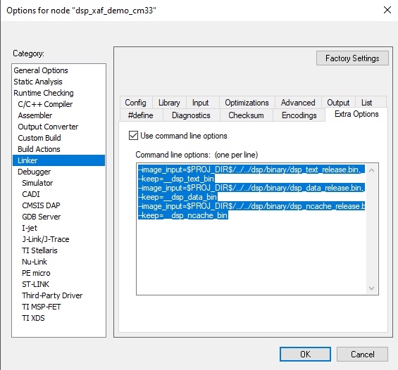
The post build scripts create the DSP images. For details, see Makefile.include in any DSP example. To reduce the image size and make image copy more efficient, they are split into SRAM part; TCM part, and uncached SRAM part. DSP images are set and linked into Cortex M33 side. For IAR, the linker is set in Project Options > Linker > Extra Options. For ArmGCC or Linux environment, set in any DSP example\cm33\incbin_gcc.S.
|
|
Parent topic:HiFi4 Boot Loader and Memory Map
Linker and Memory Map
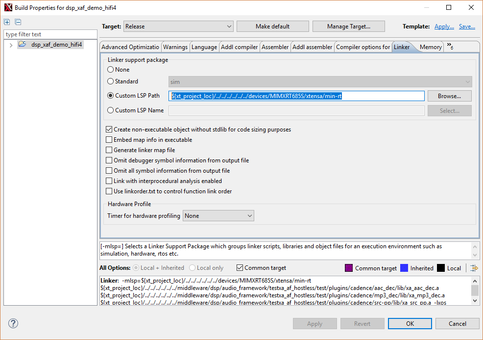
When importing the SDK DSP examples, by default the mode is set as Release. The default mode means that the images must be built in Release mode with ‘min-rt’ Linker Support Package/ LSP. To double-check, open SDK DSP examples > Build Properties > Linker.
|
|
SDK provides three different LSPs.
‘min-rt’ for Release mode - ‘min-rt’ eliminates all unnecessary debug info and reduces image size.
‘gdbio’ for Debug mode - gdbio’ support standard ‘printf’/ log output back to Xtensa Xplorer debug console, as well as other debug utilities, perfect for debug purpose but not appropriate for official deployment nor loading directly from Cortex M33 side.
‘sim’ for simulations - ‘sim’ only works for software simulation and does not fit on device debugging.
The memory map is identical for different LSPs. It sits with linker scripts in SDK path\devices\MIMXRT685S\xtensa\’LSP name’\ldscripts\elf32xtensa.x. It specifies how HiFi4 DSP organizes image sections on the memory. For example:
0x0020 0000 ~ 0x0048 0000, size 2.5 M bytes, for code and data.
Stack and Heap are at the top of the segment and count top down from 0x0048 0000 to lower.
0x2400 0000 ~ 0x2400 FFFF, size 64 K bytes, for Data TCM. By default, it is empty.
0x2402 0000 ~ 0x2402 FFFF, size 64 K bytes, for instruction TCM. By default it only contains essential vectors and left around 62 K for applications.
0x2004 0000 ~ 0x2007 FFFF, size 256 K bytes. This is non-cached area for Cortex M33 and HiFi4 DSP data exchange.
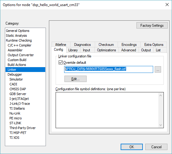
Note that both Cortex M33 and HiFi4 DSP have access to all SRAM partitions. It means that a unified memory map is necessary at system level and both cores must not affect each other’s memory map. For SDK examples, see that HiFi4 memory map starts from 0x0020 0000 and Cortex M33 side sits under this address. Using IAR environment, as an example, its memory map sits in SDK path\boards\evkmimxrt685\dsp_examples\ any example\cm33\iar\MIMXRT685Sxxxx_ram.icf.
0x0008 0000 ~ 0x0017 FFFF, for interrupt vectors and code.
0x0018 0000 ~ 0x001F FFFF, for data.
The memory map is flexible and can be adjusted as per the requirement of the application. Note that modifying the core’s memory map might affect another. Changes to both the cores must be made accordingly. For example, when allocating more SRAM partitions to DSP, you must reduce the memory taken at Cortex M33 side. Otherwise, Cortex M33 might not work properly. Also, when loading DSP image directly from Cortex M33 side, the image still sits in Cortex M33 data section before booting up. Therefore, it raises the bar for application data section requirements. You may consider running the application from FLASH.
Parent topic:HiFi4 Boot Loader and Memory Map
Cache and Data Exchange Memory Partitions
You may have noticed that HiFi4 DSP has a small non-cached area that starts from 0x20040000. The non-cached are used for data exchange between two cores. As both M33 and HiFi DSP have shared access to all SRAM partitions, shared memory access is the most effective way to exchange data between two cores. The given physical addresses are read/ written by both cores at same address, no memory mapping or address converting is required. For example, if a piece of data array is passed from Cortex M33 to HiFi4 DSP, only the start pointer and the size of the array is passed, and conversely. It is convenient for system programming and simplifies the inter-core communications.
Consider cache here. Cortex M33 has no cache, the entire SRAM is considered as its local memory. Therefore, any memory write is flushed immediately. HiFi4 has 32 K instruction cache and 64 K data cache, and both cache are enabled by default. Therefore, the memory write is not flushed immediately. To make a tradeoff between performance and IPC convenience, set the non-cached area for data exchange memory partitions.
The above memory map has specified the non-cached region, and in DSP code, and HAL functions are called to disable the cache. For details, see the audio framework example in SDK path\boards\evkmimxrt685\dsp_examples\xaf_demo\dsp\xaf_main_dsp.c. For more details about HAL cache function, see the Xtensa System Software Reference Manual, section 3.11 Cache
/* Disable DSP cache for RPMsg-Lite shared memory. */
xthal_set_region_attribute((void *)RPMSG_LITE_SHMEM_BASE, RPMSG_LITE_SHMEM_SIZE, XCHAL_CA_BYPASS, 0);
/* Disable DSP cache for noncacheable sections. */
xthal_set_region_attribute((uint32_t *)&NonCacheable_start,
                               (uint32_t)&NonCacheable_end - (uint32_t)&NonCacheable_start, XCHAL_CA_BYPASS, 0);
Note that the XHAL call sets cache attribute of the whole region/ 512 M bytes even if the set size is passed. This is also one reason why non-cached attribute is set on the overlapping SRAM address and starts from 0x2000 0000. This also distinguished the physical SRAM addresses starting from 0x0000 0000, which is cacheable area for HiFi4.
Data exchange memory partitions are flexible and can be configured as per application’s requirement. However, to mitigate the possible AHB arbitration between the two cores, use of the first eight 32 K and following four 64 K memory partitions is recommended. DSP Data TCM is also used as data exchange area for those data have high demand on timing performance. You must avoid accessing same partition at same time for frequent data exchange between two cores. You can keep one core in Sleep or Wait for Interrupt while another core operating, or set up a ping pong data exchange/ DMA such that when one core fills one partition, another core fetches another partition, and conversely.
For more details about the RT6xx memory map, see the user manual, section 2 Memory Map, and section 2.1.11 HiFi4 memory map.
Parent topic:HiFi4 Boot Loader and Memory Map
Boot or Run from Flash
Boot from Flash is straight forward when using IAR environment. SDK provides either two or four different build configurations based on the project: debug (from SRAM)/ release (from SRAM)/ flash_debug/ flash_release. Flash configurations use different memory map in project linker options. For details, see Figure 1.
|
|
To enable booting from flash, change the ISP mode/ SW5 switches on the EVK.
If using MCUXpresso/ armgcc build environment, note that by default build environment is set to boot from flash. Using MCUXpresso as an example:
Make sure to use the latest version of MCUXpresso.
Import the SDK examples.
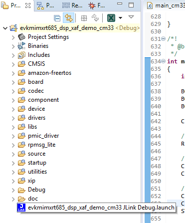
Once completed, double click the last file/ J-Link Debug.
|
|
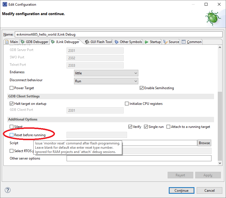
Launch to modify J-Link debugger setting.
Make sure to deselect Reset before running. This helps the flash-based program get into main function.
|
|
Make sure to:
Modify DSP_IMAGE_COPY_TO_RAM and Define to 1 in Project settings > C/C++ General > Paths and Symbols > Symbols.
Have the right compilation flag as C/C++. Compilation flags do not work on *.S files.
Have #define DSP_IMAGE_COPY_TO_RAM 1 as the first line of source/incbin.S to include the DSP binaries.
Use the correct DSP binaries at correct path (must be release binaries).
Provide the right image path to incbin.S.
To run/boot from flash, make sure that the board is set to FlexSPI flash boot mode (ISP2: ISP1: ISP0 = ON, OFF, ON).
Parent topic:HiFi4 Boot Loader and Memory Map
Parent topic:HiFi4 System Programming
Peripheral Drivers and Interrupts
This section provides information on the basics of peripheral drivers, interrupts, DMA, and how peripheral drivers work on HiFi4 DSP.
Basics
As both cores use shared SRAM and all digital peripherals, SDK drivers work the same on HiFi4 DSP. User Manual section 1.3 Block Diagram shows the system architect on this perspective. For applications, it is the same to use SDK drivers on HiFi4 DSP with Cortex M33 core. SDK has a DSP hello world UART example showing how easy to use UART on DSP side, same as Cortex M33 programming:
#include <xtensa/config/core.h>
#include "fsl_debug_console.h"
    /* Init board hardware. */
    BOARD_InitDebugConsole();
    PRINTF("Hello World running on DSP core '%s', %s_%s\r\n", XCHAL_CORE_ID);
Compare with Hello world programming on Cortex M33 side. There are two major differences:
Pin initialization is not necessary for DSP. It is doable but it is highly recommended managing all pins from Cortex M33 side to make pins all-in-one place. It is also to avoid possible conflicts when you set pins on two different cores;
Clock setting is not necessary for DSP. It is also doable but same it is highly recommended managing all clock sources all-in-one place;
Parent topic:Peripheral Drivers and Interrupts
DMA
RT6xx has two DMA controllers. Each has the same DMA request and trigger input possibilities. The two intended scenarios for their use are:
One DMA controller (DMA0) is used by the CM33, the other (DMA1) is used by the HiFi4. This case can apply to systems where there is no need to differentiate security between the CPUs or between different tasks.
One DMA controller (DMA0) is secured and has access to secure spaces and peripherals. The other (DMA1) is not secured and does not have access to secure spaces and peripherals. In this scenario, only the secure code running on the CM33 has access to the secure DMA controller. The other code and the HiFi4 share the non-secure DMA controller (if needed).
HiFi4 DSP always uses DMA1 controller. Again, it is the same to call DMA drivers at HiFi4 DSP side. The DMA destination buffer and DMA descriptor have to be in non-cached area to ensure that each transaction flushes to memory immediately. The below example code showing how to create a DMIC DMA channel:
AT_NONCACHEABLE_SECTION_ALIGN(
  static uint8_t s_buffer[BUFFER_SIZE * BUFFER_NUM], 4
);
AT_NONCACHEABLE_SECTION_ALIGN(
dma_descriptor_t s_dmaDescriptorPingpong[2], 16
);
#define DEMO_DMA (DMA1)
#define DEMO_DMIC_RX_CHANNEL DMAREQ_DMIC0
DMA_Init(DEMO_DMA);
DMA_EnableChannel(DEMO_DMA, DEMO_DMIC_RX_CHANNEL);
DMA_SetChannelPriority(DEMO_DMA, DEMO_DMIC_RX_CHANNEL, kDMA_ChannelPriority2);
DMA_CreateHandle(&s_dmicRxDmaHandle, DEMO_DMA, DEMO_DMIC_RX_CHANNEL);
Macro AT_NONCACHEABLE_SECTION_ALIGN is defined in SDK driver layer and refer to non-cached area specified by memory map.
For more details about DMA, see the User Manual Chapter 11 RT6xx DMA Controller and SDK DMA examples in <SDK path>\boards\evkmimxrt685\driver_examples\dma.
For audio peripherals/ DMIC/ I2S DMA, see <SDK path>\boards\evkmimxrt685\driver_examples\dmic and <SDK path>\boards\evkmimxrt685\driver_examples\i2s.
Parent topic:Peripheral Drivers and Interrupts
Interrupts
HiFi4 DSP has total 32 interrupts and 4 interrupt levels. Besides the first five interrupts, the rest interrupt 5 ~ 31 are multiplexed to allow more control over priorities and more general flexibility. To see the full list, see the User Manual section 8.6.3 DSP Interrupt Input Multiplexers.
It only requires few lines of code to enable an interrupt by calling XOS function calls, and peripheral controls are identical as Cortex M33 side. For example, the below code shows how to enable a UTick timer at DSP side:
First, include XOS system header files and libraries to enable necessary XOS functions.
To include libraries, go to Build Properties > Libraries > Add libraries > Select ‘xos’ & ‘xtutil’ and OK to accept.
#include <xtensa/config/core.h>
#include <xtensa/xos.h>
Set up the UTick callback and delay functions. This part is identical with Cortex M33 side. For Cortex M33 side implementation, see SDK path\\boards\evkmimxrt685\driver_examples\utick
#define UTICK_TIME_1S        (1000000UL)
#define EXAMPLE_UTICK        UTICK0
static volatile bool utickExpired;
static void UTickCallback(void)
{
utickExpired = true;
}
static void UTickDelay(uint32_t usec)
{
/* Set the UTICK timer to wake up the device from reduced power mode */
UTICK_SetTick(EXAMPLE_UTICK, kUTICK_Onetime, usec - 1, UTickCallback);
while (!utickExpired)
{
}
utickExpired = false;
}
Initialize the XOS and start UTick timer. The XOS function calls are the differences with Cortex M33 side:
/* Initialize XOS thread and start scheduler. Priority 7*/
xos_start_main("main", 7, 0);
/* Init board hardware. */
CLOCK_AttachClk(kLPOSC_to_UTICK_CLK);
CLOCK_EnableClock(kCLOCK_InputMux);
UTICK_Init(EXAMPLE_UTICK);
INPUTMUX_AttachSignal(INPUTMUX, 10U, kINPUTMUX_Utick0ToDspInterrupt);
/* To register interrupt callback */
xos_register_interrupt_handler(15, (XosIntFunc *)UTICK0_DriverIRQHandler, NULL);
/* To enable the interrupt */
xos_interrupt_enable(15);
while (1)
{
UTickDelay(UTICK_TIME_1S);
PRINTF("DSP UTICK TIMER every 1s\r\n");
}
Pay attention to the instant numbers. Pick interrupt 15, which maps to DSP_INT0_SEL10 as a L1 interrupts, lowest priority level. For more details about RT6xx HiFi4 DSP interrupt configuration, see User Manual section 51.7 Interrupt. Therefore, for Inputmux, attach UTick interrupt to 10. 15-5=10 as first five interrupts are reserved, not user configurable. To get it to highest priority level, for example L3, configure interrupt as follows.
INPUTMUX_AttachSignal(INPUTMUX, 24U,
kINPUTMUX_Utick0ToDspInterrupt);
xos_register_interrupt_handler(29, (XosIntFunc
*)UTICK0_DriverIRQHandler, NULL);
xos_interrupt_enable(29);
kINPUTMUX_Utick0ToDspInterrupt specifies DSP interrupt multiplexing value. It has been defined in SDK and matching User Manual section 8.6.3 DSP Interrupt Input Multiplexers.
For more details about XOS interrupt handling, see the Xtensa XOS Reference Manual Chapter 18 Interrupt and Exception Handling, and Chapter 26 Interrupt Handler Restrictions.
Parent topic:Peripheral Drivers and Interrupts
Complete Example
To present better how peripheral drivers work on HiFi4 DSP, below list a bare-metal DSP example program that transfers data from DMIC to codec on RT6xx EVKs. The full workspace located in <SDK path>\boards\evkmimxrt685\dsp_examples\audio_demo_bm. This example is derived from Cortex M33 driver <SDK path>\boards\evkmimxrt685\driver_examples\dmic\dmic_i2s_dma with below slightly modifications to adapt to HiFi4 DSP.
Move DMA buffer and descriptors into non-cached memory partitions;
Using DMA1 for DSP;
Calling XOS functions to enable interrupts.
This example does not contain any pin mux initializing or clock configurations. See the above Cortex M33 example dmic_i2s_dma to set up Cortex M33 side. Once Cortex M33 side ready, this example is compiled and run same as any other SDK DSP examples.
Connect headphone/earphone on audio out of the board, speak on DMIC, or play song nearby the DMIC, you can hear sound on the left channel of headphone/earphone.
/* Start XOS */
xos_start_main("main", 7, 0);
/* Disable DSP cache for noncacheable sections. DMA MUST run on none-cacheable/ cache bypass area*/
xthal_set_region_attribute((uint32_t *)&NonCacheable_start,
                           (uint32_t)&NonCacheable_end - (uint32_t)&NonCacheable_start, XCHAL_CA_BYPASS, 0);
xthal_set_region_attribute((uint32_t *)&NonCacheable_init_start,
                           (uint32_t)&NonCacheable_init_end - (uint32_t)&NonCacheable_init_start, XCHAL_CA_BYPASS,
                           0);
PRINTF("Configure DMA\r\n");
/* DSP_INT0_SEL18 = DMA1 */
INPUTMUX_AttachSignal(INPUTMUX, 18U, kINPUTMUX_Dmac1ToDspInterrupt);
/* Map DMA IRQ handler to INPUTMUX selection DSP_INT0_SEL18
 * EXTINT19 = DSP INT 23 */
xos_register_interrupt_handler(XCHAL_EXTINT19_NUM, (XosIntFunc *)DMA_IRQHandle, DMA1);
xos_interrupt_enable(XCHAL_EXTINT19_NUM);
/* The rest DMA & DMIC operations are identical with CM33 side */
Parent topic:Peripheral Drivers and Interrupts
Parent topic:HiFi4 System Programming
Messaging Unit, Semaphore, and IPC
Message Unit/ MU and Semaphore/ SEMA42 are essential for DSP programming. The inter-core communications a.k.a IPC on RT600 is based on MU and SEMA42. SDK provides three simple examples about standalone MU and SEMA 42. SDK path \boards\evkmimxrt685\dsp_examples\mu_interrupt, mu_polling, and sema42. These bare-metal examples show how IPC work between two cores. Furthermore, the audio framework demo/ SDK path \boards\evkmimxrt685\dsp_examples\xaf_demo is complete. It uses rpmsg_lite as IPC protocol, which based on MU to transfer messages between the two cores.
First Cortex M33 side initializes rpmsg master, main_cm33.c in app_task()
g_my_rpmsg = rpmsg_lite_master_init((void *)RPMSG_LITE_SHMEM_BASE, RPMSG_LITE_SHMEM_SIZE, RPMSG_LITE_LINK_ID, RL_NO_FLAGS);
  g_my_queue = rpmsg_queue_create(g_my_rpmsg);
  g_my_ept   = rpmsg_lite_create_ept(g_my_rpmsg, LOCAL_EPT_ADDR, rpmsg_queue_rx_cb, g_my_queue);
Rpmsg initialize MU interrupts for MUA/ master in rpmsg_platform.c platform_init_interrupt()
/* Register ISR to environment layer */
env_register_isr(vector_id, isr_data);
env_lock_mutex(platform_lock);
RL_ASSERT(0 <= isr_counter);
if (isr_counter == 0)
{
    MU_EnableInterrupts(APP_MU, (1UL << 27U) >> RPMSG_MU_CHANNEL);
For DSP side, it also initializes rpmsg client and tries to hook with the master, in xaf_main_dsp.c:DSP_Main()
/* Initialize standard SDK demo application pins */
my_rpmsg = rpmsg_lite_remote_init((void *)RPMSG_LITE_SHMEM_BASE, RPMSG_LITE_LINK_ID, RL_NO_FLAGS, &rpmsg_ctxt);
while (!rpmsg_lite_is_link_up(my_rpmsg))
{
It has rpmsg porting as well, initialize MU interrupts for MUB/ client in rpmsg_platform.c platform_init_interrupt() and enable it in platform_interrupt_enable()
xos_register_interrupt_handler(6, MU_B_IRQHandler, ((void *)0));
xos_interrupt_enable(6);
Once they hooked up both sides are ready for message exchange. SDK defines various SRTM message structures to pass the commands/ messages. In SDK example, it shows how to pass an MP3 decoding message, a AAC decoding message, a DMIC recording message and so on. Using MP3 decoding message as an example, It fills SRTM structure with input buffer address pointer, input buffer size, output buffer address pointer, output buffer size and so on. And then calling rpmsg to send it to DSP and waiting for the response.
rpmsg_lite_send(g_my_rpmsg, g_my_ept, g_remote_addr, (char *)msg, sizeof(THE_MESSAGE), RL_BLOCK);
rpmsg_queue_recv(g_my_rpmsg, g_my_queue, (unsigned long *)&g_remote_addr, (char *)msg, sizeof(THE_MESSAGE), len,
                 RL_BLOCK);
DSP side listens to rpmsg event.
my_ept = rpmsg_lite_create_ept(my_rpmsg, DSP_EPT_ADDR, my_ept_read_cb, (**void** *)&rpmsg_user_data, &my_ept_context);
Once received, it handles message and proceeds the command. For MP3 decoding case, it decodes the MP3 data in the input buffer, and flushes the output buffer. It also fills out the SRTM message structure with actual read data size and actual write data size, and eventually sends the response message back to Cortex M33 side.
/*Send response message*
    /rpmsg_lite_send(my_rpmsg, my_ept, remote_addr, (**char** *)&msg, **sizeof**(THE_MESSAGE), RL_DONT_BLOCK);
For this example, DSP is considered as a coprocessor and rpmsg has been used for a light-weight IPC for both cores. All modules are open-sourced and could be easily adapted to whatever application needs.
Parent topic:HiFi4 System Programming
NatureDSP Library
To facilitate application development on RT6xx HiFi4 DSP, NXP licensed NatureDSP signal processing library and embedded as is in source code format. It is found at <SDK path>\middleware\dsp\naturedsp_hifi4.
This is an extensive library, containing the most commonly used signal processing functions: FFT, FIR, vector, matrix, and common mathematics. API and programing guide in.\doc\NatureDSP_Signal_Library_Reference_HiFi4.pdf, and performance data in .\doc\NatureDSP_Signal_Library_Performance_HiFi4.pdf
As this is a huge library, it is impossible to build an all-in-one example on the RT6xx hardware. Fortunately, this library is in source code format and each function/ filter are wrapped in standalone source file. They could be integrated to any application as needed.
Parent topic:HiFi4 System Programming
System Optimization
Performance and power efficiency are key for embedded systems. The following sections list some tips and best practices for system optimization from this perspective.
Profiling
The Xtensa Xplorer IDE tool can run software simulation and profile the application directly. Both simulation and profiling are cycle accurate. This is convenient for algorithm or heavy application developers.
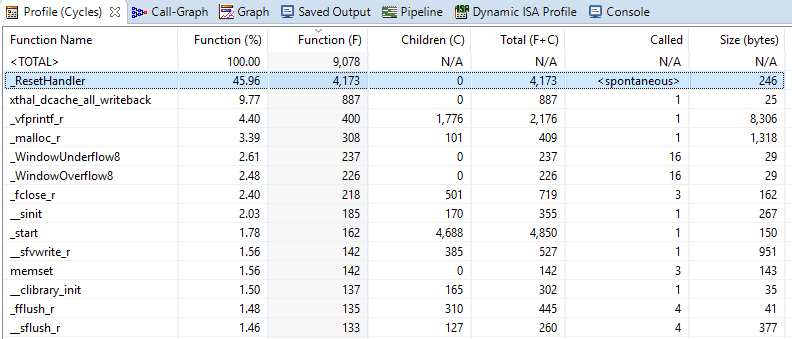
Figure 1 shows profiling result of the helloworld program on simulation console.
|
|
Figure 1 shows the profiling chart, partially.
|
|
The generated license file only supports debug/run on the RT6xx device target. It does not support software simulation/Xplorer ISS. If there are special requirements to run the software simulations, contact Cadence directly.
It is also common to measure exact cycle counts for specific processing/ timing measurements. The following is an example code to show how to do the cycle counts.
/* Cycle counts inline function */
static unsigned long inline get_ccount(void)
{
    unsigned long r;
    __asm__ volatile ("rsr.ccount %0" : "=r" (r));
    return r;
}
tic = get_ccount();
processing_function();
toc = get_ccount();
printf("Processing takes %d cycles \r\n", toc - tic);
Parent topic:System Optimization
Using Local Memories
RT6xx HiFi4 DSP has 64 K data TCM and 64 K instruction TCM. The TCM is filled with less than 2 K of kernel vectors and the rest is available for application needs. They are the fastest RAM available with no access latency, and can improve critical data/ instruction performance considerably. Consider using TCM as much as possible.
To program code/ data to TCM area:
Define macros for sections in TCM. Reuse existing .drm0 and .iram0 sections. Both sections are default TCM sections for every Xplorer project/ memory map. The following are the sections in fsl_common.h.
#define DRAM0_DATA __attribute__((section(".dram0.data")))
#define DRAM0_BSS __attribute__((section(".dram0.bss")))
#define IRAM0_TEXT __attribute__((section(".iram0.text")))
#define ALIGNED(alignbytes) __attribute__((aligned(alignbytes)))
Use macros to declare code and data to be placed in TCM. The data and bss/ uninitialized data are different sections. The following is an example for an FFT function call.
DRAM0_DATA const static int32_t fft_in_ref[FFT_LENGTH] = {
DRAM0_DATA const static int32_t fft_out_ref[FFT_LENGTH] = {
DRAM0_BSS static int32_t fft_out[FFT_LENGTH];
IRAM0_TEXT int TEST_FFT()
{
  …
        fft_cplx32x32(fft_out, fft_in, FFT_HANDLE, 3);
  …
}
The TCM addresses start from 0x2400 0000, which is too far away to main(). Therefore, the project enables long calls to ensure that main() is able to call sub functions. To enable, select Build Properties > Optimization > Enable long calls and select the Yes checkbox. Alternatively, add -mlongcalls to the compiler flags.
Parent topic:System Optimization
Power Efficiency
RT6xx HiFi4 DSP has been equipped as a powerful processing core that can run at 600 MHz, but it may not be necessary at all time. It is always recommended to optimize the power efficiency at system level.
Voltage level and core frequency have huge impact on the power efficiency. Using FFT processing as example, continuous FFT may take ~130 mW at Vddcore 1.1 V / 452 MHz, and ~4 mW at Vddcore 0.7 V / 29 MHz, at room temperature. Profile or do cycle counts for software workload. If it only requires 300 MHz at peak, then the run at full power is not required. Instead, it can run with Vddcore 0.8 V 300 MHz. For more information on the Vddcore and DSP frequency operating conditions, see any dsp example\cm33\pmic_support.c BOARD_SetPmicVoltageForFreq(), or see the data sheet, section 13.1 General Operating Conditions.
Some other tips for better power efficiency:
Turn off DSP/ set DSPSTALL, if needed.
If possible, make DSP clock adapts to its workload.
Call XT_WAITI when DSP is in while loop waiting for interrupt. Similar to Arm side __WFI(), it suspends some processor operations to reduce the power consumption.
#include <xtensa/tie/xt_interrupt.h >
 extern void XT_WAITI(immediate s);
The immediate value passed is the interrupt level or lower to be IGNORED. For example, if you call XT_WAITI(2) both L1 and L2 interrupts are ignored and only L3 interrupts can wake up DSP.
Current can further reduce when clocks are turned off to unused memory partitions. For more information, see User Manual 4.5.5.13 DSP SRAM access disable, Register SYSCTL0_DSP_SRAM_ACCESS_DISABLE.
PLLs consume power. Consider FFRO for low-power use cases.
Parent topic:System Optimization
Parent topic:HiFi4 System Programming